JustForex
Loading recent posts...

Sep 2, 2012

SONY Tab 20 Home Tablet


Japanese giant electronics and entertainment company SONY apparently thinks that we should all have a home tablet next to our PC, mobile multimedia and communication tablet, mobile notebook workstation and big screen smartphone.

The IT companies are trying hard to convince us we need all of these, and SONY’s new Tab 20 / home tablet concept made us wonder what its primary use or reason for being is. The best explanation we have for it is that this is basically a huggable AIO computer that has a small battery to allow you to carry it from one room to another. The SONY Tab 20 is a 20” tablet with a 10-point multitouch display featuring a rather modest 1600 by 900 pixel resolution that doesn’t exactly fit with the usage model, SlashGear reports. When you’re holding it on your lap while sitting on the bed, you actually hold it quite close and pixels will be somewhat visible. If 10” tablets get FullHD screens, we believe SONY’s Tab 20 should have at least the same 1920 by 1080 pixel resolution.

Behind the rather huge 20” screen there is a normal and quite powerful PC configuration that will allow you to fully enjoy Microsoft’s Windows 8 operating system and the whole x86 software base. A normal AIO system normally sits on a table and you can’t carry it with you to another room, and you’re forced to shut it down before you plug it out of the power socket. With SONY’s Tab 20, you can take the system to any room and place it virtually anywhere without worrying about shutting it down before yanking the cable out of the wall socket.


SONY Tab 20
Images credits to SlashGear

Intel Xeon Phi Barely Equals AMD VLIW Radeons


Intel’s work on the Larabee project and succeeding Xeon Phi accelerator cards has costed the company billions of dollars and lasted for almost a decade. Now the architecture is finally ready to fight for a place on the GPU compute market.

During this year’s Hot Chips conference in Cupertino, California, the world’s largest semiconductor company has shared the final details on the Xeon Phi cards and it seems the company has achieved a lot for a first generation product. On the other hand, not all is rosy for Intel and its Xeon Phi project. Intel’s problem is best described by its own slides during the presentation as the company is actually now comparing its new and very advanced architecture with last year’s technology from AMD and Nvidia and still can’t show any impressive results. It is widely known that AMD’s VLIW architecture was quite handicapped when it came to GPU compute work and Nvidia’s 2090 accelerators, while being considerably better, were launched a year ago.

Even so, these are the only examples Intel has found in the famous Top500 list of supercomputers that could allow it to present its new Xeon Phi cards in an acceptable light. Intel’s performance per watt improvement measures just 0.7% when compared with a server using VLIW AMD cards and 9% when compared with a server using Nvidia’s Tesla 2090 cards. We’re quite surprised AMD has the better solution when it comes to GPU compute and performance per watt, especially because we’re talking about a VLIW design, but overall Intel’s Xeon Phi is quite disappointing. Despite the company has a much better manufacturing technology as the Xeon Phi chips are made using 22nm transistors and the world’s best software optimization and compiler support, but the results are only comparable with AMD’s and Nvidia’s last year’s tech.

Intel Xeon Phi Processor
Image credits to slashgear

Intel Xeon Phi Hot Chips 2012 Presentation
Image credits to Intel

HP Stunning SpectreXT TouchSmart Ultrabook


HP decided to surprise the UltraBook fans with an incredibly well built and well featured mobile device at the IFA 2012 event in Berlin, Germany. The new mobile system features the first ThunderBolt port on a HP UltraBook and it’s the first time the company has used a 1080p IPS screen on such a design.

We’re very glad HP has decided to equip its new UltraBook with such high end features, but we’re even more impressed with the fact that it also comes with an incredibly strong and good looking magnesium alloy body. The laptop is only 17.9 millimeters thick (0.7”), but weighs in at 4.77 pounds (2.16 Kg) and that’s a bit heavier than Lenovo’s S series.

It is build using Intel’s Ivy Bridge and comes with two USB 3.0 ports and an SD cards reader along with a long list of pre-installed productivity software such as Adobe Photoshop Elements 10, Adobe Premiere Elements 10, sMedio 360, HP Connected Music, Absolute Data Protect, two years of Norton Internet Security and others.


HP SpectreXT TouchSmart Ultrabook with ThunderBolt, FullHD IPS, Touchscreen, USB 3.0 and a 17.9 mm magnesium body
Images credits to HP

AMD Different CPU Design Method Experiments [Updated]


AMD has decided to concentrate on the bulk manufacturing process instead of the usual Silicon-on-Insulator (SOI) that has been the company’s main technology for the past eleven years.

Back in 2001, AMD’s Palomino processors, or the famous AthlonXP as most of us knew them, were imbued with IBM’s SOI technology to help achieve higher working frequencies by lowering the amount of current leakage and power consumption. When designing a high frequency microprocessor, the architect is not really concentrating on lowering the power consumption. Some of the internal units that are literally getting very hot when heavily in use could pose a problem to the chip’s overall stability and ability to function. Therefore the designers usually take the decision to move their position to a somewhat “cooler” are of the chip. When designing a microchip with tens of millions of transistors or even billions, moving around some of the functional units might make the overall die size of the chip a whole lot bigger.

Back when Intel and AMD were fighting head to head for the absolute performance crown, some concessions about the die size and power consumption were made. Basically the companies thought it was alright to have a 140 watts CPU TDP if that was what it took to win the benchmarks. The same goes for a 10% to 20% bigger die size. This was back in the days when AMD has its own foundries and all the costs were managed by the company itself, but now that AMD is paying TSMC or GlobalFoundries for manufacturing their designs, the bigger die size would come with a significant increase in costs per chip. Now the company is working with different foundries that are mostly using bulk manufacturing process and have various chip design tools at their disposal and it believes all this diversity comes with impressive potential. Real all about these impressive AMD simulations and potential improvements in Part 2 of our AMD report that's coming later this week.

AMD Phenom CPU Die
Image credits to AMD

Manually designing some of the functional units on a microprocessor was possible and was a method often used back when a CPU had 100,000 or a million or tens of millions of transistors.

Now that CPUs are going well beyond the 2 billion transistors mark, moving millions of transistors around on the design is a very complex operation that usually leads to a great increase in die size. Also, hand drawing the layout is a very complex operation that can be heavily optimized by specialized software. When transistor count is the criteria, the most popular complex chips are the GPUs that have reached and surpassed the 4 billion transistors mark back in 2011 with AMD Tahiti design. Since Nvidia’s and AMD’s GPUs are made at TSMC and both designers pay the foundry for each processed silicon wafer, it is very important that the make as many GPUs per wafer as possible.

For this, each foundry usually provides its customers with automated microchip design tools that will take a design and rearrange the units and the transistors in a manner that’s best suited for that specific manufacturing technology. This way, the specialized software makes the chips much smaller and also makes sure that everything works fine. The design software usually goes for two things: the tightest design when everything works properly. When making networking or DPS processors, this is probably the best approach to get as much CPU dies per wafer and, therefore the lowest manufacturing costs per chip. One thing that might not appeal to enthusiasts is that these chips work at much lower frequencies than the ones with manual intervention on the die design.

Basically AMD’s Bulldozer might not easily reach 2 GHz, if its die design would be so crammed. At 2 GHz, the internal units would likely work fine, but raising the frequency any higher would make the “hot” units give out errors or leak electrons that would affect the surrounding transistors.

AMD Hot Chips 2012 Slide
Image credits to AMD

During this year’s Hot Chips conference in Cupertino, California, AMD has presented what they’ve been able to achieve by using automated design tools (software) to rearrange the units inside its Bulldozer processors.

Like we’ve just explained above, such a design “optimization” is mainly used for very big chips such as GPUs and readers should keep in mind that the fastest GPUs today hardly reach above 1.2 GHz in normal conditions. Such a frequency would be catastrophically low for a CPU like AMD’s Bullzoder and despite the lower manufacturing costs and power consumption, not many would be interested in powering a personal computer with something like this. The thing is that the Bulldozer die doesn’t have as many transistors as a Tahiti dies and as such will be able to reach much higher frequencies than the GPU dues to having a smaller and less complex die with a more modest power consumption.

Now we have a 2 GHz Bulldozer that has a small and economic die size and an improved power consumption level. Interestingly enough, AMD is not aiming for a complete overhaul of its CPU die design. Just like shown at the 2012 Hot Chips conference, the company is only redesigning parts of the CPU using the automated design tools. The units in question become much smaller and manifest lower power consumption. AMD is showing a floating point unit (FPU) in the graphs made public at Hot Chips. The unit has been greatly reduced in size by using a different design solution (software using a High Density cell library). A 30% reduction in die area is touted along with a 15% to 30% power consumption and these are results usually obtained by moving manufacturing from one node to another. Getting a design from 32nm to 28nm manufacturing could take a whole year or even more.

Adding to the expected 20% ~ 30% die shrink and power consumption reduction that comes with such a move an additional 30% shrink and power improvement due to a tighter design would result in impressive results. Such results would be comparable with a move to 20nm manufacturing. The unknown is the frequency of such a design, but the company could opt for a differentiated clock design where some units work at a certain frequency and other units have a much higher functional frequency. Extrapolating from AMD’s graphs, we could imagine a CPU that has more FPUs that are all kept fed by very fast dispatch units with efficient branch prediction. It is all about balance and getting the right recipe, but what AMD is basically saying is that they are working with many solutions that offer good improvements and that combined will offer impressive results.

AMD Private Meeting Highlights: Yes to Tablets, No to Ultrabook Alternative


Being one of those lucky enough to land a one-on-one briefing with AMD at IFA 2012, I got the inside scoop on quite a few things, from laptops to tablets and the processors used in them.

It was actually surprising to learn that AMD was going to focus on tablets during the meeting, rather than ultrathin laptops and notebooks. Nevertheless, that is what happened. There are some things we can’t talk about just yet, but we have free reign on just as many subjects, if not more. To start off, AMD isn’t going to follow the same pattern that the rest of the IT industry adopted in regards to the tablet market. For those who don’t know what we mean, many companies released a sort of test product before entering the segment, some after taking months to “study marketing conditions.”

AMD took its time not because it didn’t believe in the idea, but because it wanted to be sure it could make an impact, which means that they will push fast and hard. Bulldoze the segment as it were. Of course, it remains to be seen if they succeed in entering the “sweet spot” of the tablet market from the start. Our guess is that they will, because Trinity, and the work on the part of the HSA Foundation, is significant in its thoroughness. Besides, APUs have always been about performance at a low price and reduced power draw, and reports have been roaming the web about a certain Hondo low-power 40nm chip with 4.5W power draw. Setting aside what we know right now, some, like Fudzilla, think this is the next-generation mobile chip, while others still believe Hondo to have been cancelled a while ago.

That said, AMD talked about the ultrathin notebook segment and what plans it has for it. It turns out that there won’t be an ultrabook alternative in the strictest sense. I asked them if they thought about a counter-brand, and they said that they don’t see a need for it, especially since the normal term “ultrathin” defines the same sort of product but is not as restrictive (the screen size can go above that of ultrabooks, the feature set can vary more, etc.). Verily, it may even be a good idea to go this route for a very uncanny reason: promoting something as an “alternative” to ultrabooks would immediately cause prospective buyers to think the AMD-based devices are just as unimpressive and/or not worth buying as them. 

We aren’t saying that ultrabooks are bad. The Acer Aspire S7 would have our hide if we did. Nevertheless, all market analyst firms are in agreement that sales have consistently failed to impress. Thus, it might be good for AMD to have nothing to do with a product type that is dragging its feet one year after it was supposed to win back the consumer base stolen by tablets. On that note, HP is, at this point, the only PC maker with a special “brand” for AMD ultrathins (Sleekbook).

AMD logo
Image credits to AMD

HTC Accord Windows Phone 8 Device


Rumors on the upcoming HTC Windows Phone 8 devices started to pour in a few months ago, though the Taiwanese company has yet to confirm any of these speculations.

Although it’s not yet clear how exactly HTC plans on taking Nokia on the Windows Phone market, it appears that new info on one of the unannounced WP8-based handsets has just emerged online. A photo of the alleged HTC Accord, one of the Windows Phone 8 smartphones that leaked for the first time back in June, was recently published by an XDA Developers forum member via Twitter. Along with the said press photo, several specs of the HTC Accord have been unveiled also, then again there have been no confirmation from the handset maker so far.

Today, a new render of the purportedly HTC Accord has been published by the same XDA Developers forum user. It appears that this is as schema of the phone, and looks the same as the device leaked in the first picture. According to the latest hearsay, HTC plans to unveil three Windows Phone 8 smartphones in the third week of September, the Zenith, Accord and Rio. HTC Accord is a mid-range WP8-powered handset, the Zenith will be the company’s new Windows flagship smartphone, while the Rio is said to be the cheapest in the series.

Hardware-wise, the Accord is expected to be equipped with a dual-core Qualcomm Snapdragon S4 processor clocked at 1.5 GHz, a decent 4.3-inch HD (720p) Super LCD2 capacitive touchscreen display, as well as an impressive 8-megapixel rear camera with full HD (1080p) video recording. We also know the smartphone will pack 8GB or 16GB of internal memory, which can be further expanded via microSD memory card. NFC (Near Field Communication) technology will be integrated as well. No other details have been leaked for the moment, but we will keep a close eye on this one, so stay tuned for more updates.


HTC Accord
Images credits to Football4PDA

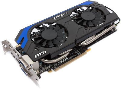
MSI Nvidia GeForce GTX 660 (GK106) Power Edition Video Card


We’ve already reported about the Nvidia GK106 GPU here, but it seems like we were somewhat right and, if the GPU has 1152 CUDA cores on the semiconductor die, the retail cards will not come with all the processing units enabled.

There is the unlikely possibility that the GK106 really has only 960 CUDA cores inside, like depicted in MSI’s marketing material on its GTX 660 Power Edition card. The most likely scenario is that Nvidia will eventually stop using the GK106 for the GTX 660 Ti cards and go for the cheaper and cooler GK106.

We will not have to wait too much to receive official confirmation from Nvidia as the GK106 and the GTX 660 video card will be officially launched next week.


MSI Nvidia GeForce GTX 660 Power Edition Video Card
Images credits to obr-hardware

How Thin the iPhone 5 Really Is? This is 3GS, 4S and Next iPhone 5 Comparison


The French are at it again with a new set of images that aim to give us a good picture of what the next iPhone will look like.

Nowhereelse.fr has posted images showing a comparison between the iPhone 4S, the iPhone 3GS, and the next-generation iPhone’s chassis. Sandwiched between its older counterparts, the iPhone 5 is notably thinner and svelter. This achievement was possible thanks to Apple’s machining process behind the unibody enclosures for its popular products. This time around, they’ve used it on the iPhone too, not just Macs.

Apple is expected to lift the cloth off this shiny new product next week, during a press event that is rumored for September 12. Physical availability of the handset is expected around September 21. The consensus is that the iPhone 5 will have a bigger display (4 inches on the diagonal), a smaller dock connector and some relocated ports and connectors. The camera modules should also be enhanced.

iPhone 3GS, 4S and Next-generation iPhone 5 thin comparison
Image credits to nowhereelse.fr

Twitter Delicious Facebook Digg Stumbleupon Favorites More

 
Design by Free WordPress Themes | Bloggerized by Lasantha - Premium Blogger Themes | coupon codes
`