JustForex
Loading recent posts...

Apr 27, 2012

iPhone 5 "Spotted" By Enthusiasts in WWDC 2012 Logo


There’s a five (5) in the WWDC 2012 Apple logo if you look from just the right angle, many Apple enthusiasts agree.

However, by connecting the squares you also get a two (2), and even an eight (8) if you look at the bigger picture.

Despite the fact that Apple does hide clues in its logos occasionally, we have every reason to believe this is nothing more than simple speculation coming from people who love Apple products a tad too much.

So much that they’ll see an iPhone in everything, pretty much like those people who see the Virgin Mary in their coffee dregs.

Not to say there isn’t an offset chance Apple will announce its new iPhone at the WWDC 12 opening keynote, but the chances are so slim it’s not even worth bothering our heads with it. Here’s why.

Apple’s press release confirming the time and place for this year’s developer conference specifically mentions all of the major activities surrounding iOS and Mac OS. And that’s pretty much it - no hardware stuff. Just software!

“We have a great WWDC planned this year and can’t wait to share the latest news about iOS and OS X Mountain Lion with developers,” said Philip Schiller, Apple’s senior vice president of Worldwide Marketing. “The iOS platform has created an entirely new industry with fantastic opportunities for developers across the country and around the world.”

Apple typically doesn’t lay out its roadmap when they’re preparing to announce something big. Whenever Apple announces a major new product or refresh, the press invites generally say “let’s talk iPhone,” or “back to the Mac.”

After all, it’s misleading to suggest a complete focus on software and then BOOM! iPhone 5. Not that it wouldn’t impress people, we have to agree.

And there’s a slim chance Apple will announce some new hardware at the opening keynote. But there’s a bigger chance those will be the new Macs, not the new iPhone.


Entry-Level Sony Xperia Tapioca (ST21i) Photos and Specs Leak


We have new info on Sony’s Android roadmap for 2012. We already know that the Japanese company plans to release several Android smartphones by the end of the year, along with at least a few carrier-bounded variants of these devices.

Leaked back in January, Sony’s roadmap includes names such as Xperia S, Kumquat, Nypon, Pepper, Hayabusa, Tapioca and others. Some of these smartphone have already been announced and released on the market, but most of them are expected to arrive in Q2/Q3 2012.

We already reported today on the recently leaked Sony LT29i Hayabusa, which is slated for a June release. Apparently, this will be Sony’s new Android flagship smartphone and will feature a 1.5 GHz dual-core Snapdragon S4 processor and a 13-megapixel rear camera.

However, we’ve just received new info on another device that’s been part of Sony’s roadmap for this year, the ST21 Tapioca.

Opposite to Sony LT29i Hayabusa, Tapioca is one of the company’s low-end Android smartphones, so don’t expect anything outstanding from this one, except maybe the price tag (hopefully).

There is some good news though, as Sony ST21i Tapioca is said to be powered by Google’s Android 4.0 Ice Cream Sandwich operating system. Obviously, it will also provide users access to more than half a million apps and games via Google Play store, formerly known as Android Market.

Even though the smartphone is codenamed Tapioca, it’s likely to be launched under a different name. According to TechBlog, the smartphone features a decent 3.2-inch capacitive touchscreen display that supports 320 x 480 pixels resolution.

On the inside, Sony ST29i will be equipped with an 800 MHz single-core processor, which will be complemented by an Adreno 200 graphics processing unit and 512MB of RAM. In addition, the handset is said to pack a 3-megapixel rear camera and a 1460 mAh Li-Ion battery.

There are no details on the phone’s price and availability, but rumor has it the Tapioca might be launched on the market as early as July.


Script: G5 Framework


The G5 Framework is a front-end framework for quickly deploying a basic website front-end, on which to add content and modify along the way.

G5's main role is to speed up development, to reduce time with repetitive tasks by providing a batch of top-of-the-line tools out of the box. Whoever created more than 2-3 web projects can see the bright part in this philosophy.

By not spending a huge amount of time in rounding up front-end utilities, which most developers end up modifying anyway to fit their overall architecture and design style, a developer has more time to spend on creative work, adding content, features or just testing.

The G5 framework is basically a project wireframe (skeleton) on which other tools can be added.

By default it comes packed with jQuery, Modernizr, IE6 fallbacks, CSS3 templates, a grid system, SEO tools, a modal windowing system, tooltips, an image slider for featuring content, and many more other features.

Download the G5 Framework here.
The framework has bee also ported to LESS under the name G5-Less.


China Choosing the National CPU Architecture: MIPS and Alpha Seem Favorites


China’s high ranking representatives gathered at a top level meeting last month at their Ministry of Industry and IT to discuss ideas and initiatives regarding their own National CPU Architecture.

For those less familiar with processor design, the first thing on the table is the decision on the ISA. 

ISA is short for instruction set architecture and is defined by Wikipedia as:
the part of the computer architecture related to programming, including the native data types, instructions, registers, addressing modes, memory architecture, interrupt and exception handling, and external I/O. An ISA includes a specification of the set of opcodes (operating codes / machine language), and the native commands implemented by a particular processor.

ISA can be RISC or CISC, but historically RISC architectures have been the most successful.

One might say that x86 is very successful and is categorized as CISC, but today’s processors, even since the P5 times of AMD’s K6 innovative architecture and Intel’s heavy Pentium II, have been translating legacy x86 instruction into small micro-instructions or micro-ops that are executed in a quite similar manner with the RISC concept.

Practically, today’s x86 is a legacy ISA “supported” by much more innovative CPUs that have to translate the x86 commands into internal code, execute the commands and then retranslate the result into x86 compatible format.

Therefore, we’re back at RISC. It would certainly be very interesting to start developing a highly parallel architecture that supports other ISAs, just as Transmeta developed x86 over a VLIW architecture. Thus you have a huge advantage over everything that requires parallelism performance and you’re able to execute on different ISAs just as needed.

We don’t think China will want to experiment and it will rather go for a tried and true architecture. X86 is out of the question as it belongs to Intel, and Intel is not licensing it anymore; not that it ever really did.

ARM belongs to AMD Holdings and is quite tempting as it is very popular these days and can handle any project from mobile phones to servers, but we think the most likely candidates are MIPS and DEC’s Alpha.

MIPS is an ISA that has extremely good scaling, efficiency and has been proven in both tablets/mobile devices and servers. MIPS is a tempting buy for quite a lot of companies, and it is available for sale as we’ve reported in detail here.

Alpha is a legendary server-suited architecture that has ruled the first half of the ’90 and it has absolutely revolutionized the PC market too.

DEC’s design team leader Dirk Meyer joined AMD in ’96 and, in three years, using many design elements and concepts similar to the Alpha architecture, managed to build a CPU that was 40% more powerful than any other x86 CPU on the market at that time.

Alpha was unfortunately left to die and now there are no processors build on the Alpha ISA that have any degree of industry popularity.

Alpha could have practically destroyed Intel’s performance advantage if it had ever been developed for the PC market.

Compaq’s misfortune was Alpha’s misfortune: they’ve decided to phase out their Alpha servers and got fooled into investing in Intel’s Itanium architecture. The move was just as good as SGI’s Itanium ill-fated decision to scrap MIPS and go for Itanium. Compaq ended up being sold to Hewlett-Packard. The move was considered “bold” at the time but, under the disastrous management of Carly Fiorina, the HP+Compaq entity ended up having a market share smaller than DELL’s.

With no real guidance, Carly Fiorina’s disoriented HP sold all Alpha intellectual property to Intel. Intel bought everything because it knew they have much to learn from the architecture that helped AMD offer the best computing performance during the 1999 ~ 2006 period.

Having has such a great effect on everything it touched, no matter if that was Compaq, AMD, Intel or DEC, the Alpha ISA is a great candidate for China’s National CPU Architecture project.

There are many Chinese companies successfully using and integrating different ISAs.

There is the MIPS ISA developed at Loongson and Ingeniq (that we’re already reported about here).

The 1995 'Shenwei' Alpha based design currently used for military workstation, servers and supercomputers.

China’s military is also using the 'Fengtian' SPARC design.

We don’t think China will start developing an Isa from scratch and we believe they will rather go for something they’ve already tried.


Sony NEX-F3 Leaked Will Have 16.1 MP Sensor


Sony, like Nikon, is preparing to launch a new mirrorless digital camera, but at least we have a picture to show for it this time. 

Don't be fooled by our report on the Nikon D600. The photo posted there is of the D800. 

Now, though, Sony's rumored NEX-F3 has been pictured, although poorly. 

The image isn't blurry or anything, but it definitely isn't very well framed. 

Nevertheless, it will have to be enough for now, along with the few uncovered specs: a 16.3 megapixel sensor, built-in flash, a 180-degree tilting screen and the possibility to fine-tune manually-focused shots via a new peaking level feature. 

People entertaining thoughts of buying this thing will have to be careful when getting an accessory. The peripheral connector is that proprietary port Nikon came up with, not USB or anything more universally compatible.


Sony LT29i Hayabusa with 1.5 GHz Dual-Core CPU and 13MP Camera Arrives in June


Sony’s 2012 Android roadmap leaked earlier this year, but aside from the Xperia S, P and U, none of the devices listed have been announced yet.

Although we’ve already got several leaks on various Sony models that will probably make their debut by the end of the year, nothing has been confirmed yet.

One such device is the Sony LT29i Hayabusa, which will presumably be the company’s new Android flagship smartphone. The phone was initially slated for a July release, but rumor has it that the device will be released one month earlier, in June.

According to the guys over at PhoneArena, the LT29i Hayabusa boasts an impressive 4.55-inch HD Reality capacitive touchscreen display. The phone will be powered by an equally impressive 1.5 GHz dual-core Snapdragon S4 processor.

Another selling point of Sony’s top-tier device will probably be the 13-megapixel rear photo snapper, which features the innovative “HDR Video” function, improving low-light performance, autofocus, LED flash and full HD (1080p) video recording.

The phone will be only 7mm thin, though it will pack a high-capacity 2200 mAh Li-Ion battery, which will hopefully provide a longer autonomy.

In the same piece of news, Sony plans to introduce the Hayabusa in the States as well. The phone will be exclusively launched through AT&T with the codename Sony LT28at. Unlike the LT29i version, the carrier-bounded variant will come with LTE support.

Obviously, both versions will be powered by Google’s Android 4.0 Ice Cream Sandwich operating system, possibly integrated with some sort of Sony Timescape user interface.

No word on whether or not Sony will release both models around the same timeframe, or AT&T customers will have to wait a few more weeks or months in order to be able to get the Sony LT29i / LT28at. Stay tuned for more updates on the matter.


New “Dummy” GALAXY S III Pictured, It Looks Closer to the Final Design


Rumors on the upcoming release of the Samsung Galaxy S III continue to spice up our lives almost every day. 

Aside from the numerous leaks on the phone’s specs sheet, there’s also quite an impressive gallery of alleged Galaxy S III that’s been fueled by “trusted source.”

However, it appears that Samsung is safeguarding the design of its “next Galaxy” smartphone fiercely as the company has been reportedly using generic boxes for testing purposes, in order to keep the final design of its flagship device secret.

Although we already know that all photos that have been lately leaked online are simply showing some of these test sample units, which have nothing to do with the final version of the Galaxy S III, at least we get to learn the phone’s specs sheet and its capabilities.

We’ve already seen a couple of Galaxy S III variants, so bear with us for one more photo of the alleged “next Galaxy” smartphone, which is set to be unveiled on May 3, in London.

The guys over at PhoneArena recently received an image from one of their tipsters who claims this is the highly-anticipated Samsung Galaxy S III.

Unlike any of the previous photos, this one seems to be in line with the sketch spotted in the official manual leaked yesterday.

The purported Galaxy S III device shown in this photo features a physical home button and two capacitive touchscreen keys. 

The home button is a hot subject for Samsung fans as some of them would prefer that the company launches a Galaxy S III with only on-screen button, while others would like to see the phone featuring a physical button.

Even though there’s no telling exactly what the Galaxy S III will look like, the device in the latest photo might seem awfully close to the final design.


G.Skill Hosts Extreme Overclocking Competition


Enthusiast memory manufacturer, Taipei-based company G.Skill, has just announced on HWBOT's official page that they’d be hosting an overclocking competition having memory kits as prizes.

This is following the release of the new extreme DDR3 lineup, called TridentX. The extreme overclocking contest will be held at HWBOT, the widely recognized authority in the overclocking field.

The G.SKILL CUP OC competition begins on May 1st and will run until May 30th.

There will be three competition stages : 

Stage I: Max Memory Clock (the highest memory frequency achieved);

Stage II: SuperPI 32M on the new Ivy Bridge platform (with no limit on the frequency);

Stage III: Maxi  IGP result in Futuremark’s 3DMark06, as memory bandwidth plays the most important role in the iGPU performance.

We wish everybody good luck and we’ll welcome any pictures or small films with the results from the event.


Nvidia Prepares Faster Tegra 3 Version


Nvidia is reportedly working on an improved version of its very popular, but already semi-obsolete Tegra 3 mobile chips.

Tegra 3 was quite an unlucky and short-lived chip. While it performed very well and still does, it came into the market together with the ARM Cortex A15 designs.

Nvidia’s penta-core chip is a very innovative and well-performing chip. It has very low power feature for a chip its size and Nvidia practically delivered on everything it has promised about it.

The market of mobile chips moves much faster than the CPU or GPU market that Nvidia has been accustomed with. In a very short period of time they launched the Tegra 3, but while they were working on this 4+1 novel architecture, the other ARM player on the market was busy designing Cortex A15-based designs.

In the mobile software domain, and in the usual desktop PC domain for that matter, finding applications that can use four cores is quite difficult. Maybe because of the huge software diversity, the desktop PC side has a lot of practical examples, but in the Android world that doesn't happen too often.

The CortexA15 dual core design offers the same, if not more performance than Tegra 3, while not needing a special quad treading software optimization. Every single threaded or dual-threaded application will output a more smooth result on a Cortex A15 chip than on Nvidia’s Tegra 3 as we’ve already reported here.

This is exactly why Nvidia is trying hard to improve the performance of its Tegra 3 chip to keep the pace with the dual core Cortex A15 designs and to get better single-threaded performance.

Rumor has it that maybe only one of the cores inside the AP37 chip will be able to clock to the high 1.7 Ghz, but that would be a nice 14% speed improvement, if true.

The big step will be related to the GPU performance. Nvidia will probably clock its iGPU higher in the Tegra 3 chip and it’s shooting for a 25% performance increase.

Therefore, we can see that these improvements are highly interlinked. Nvidia wants a faster GPU, because many devices are now going to use Full HD screens, and the standard Tegra 3 is tailored only for the 1366 x 800 pixel resolution.

The AP37 will be made specifically to drive screens with a 1920 x 1080 resolution, or maybe even 1920 x 1200, but a faster GPU needs a tad faster CPU to really show that 25% improvement – hence Nvidia’s 1.7 GHz main CPU clock speed.


Acer’s V3 Ivy Bridge Laptop Spotted


Acer is reportedly preparing to launch the Acer V3 line of laptops in Japan. The V3 will come with 8GB of DDR3 memory and a plain 15-inch glossy screen.

As usual, Japan gets all the goodies. It’s not that much that they’re closer to Taiwan and China, as it’s about the fact that the average income is so much higher, that everything new is selling for around double the price, and every device manufacturer wants a taste of those profits.

Acer is preparing to launch a more down-to-earth laptop using Intel’s new Ivy Bridge architecture.

This is a regular 15” laptop with a wide 15.6” screen size, sporting a regular 1366 x 768 HD resolution.

It is powered by Intel’s Core i7-3612GQ processor. We’ve practically never heard of this GQ version. Surprisingly, Bing and Google return zero results when we try to search for it.

We believe it’s likely related to the Core i7-3612QE and the Core i7-3612QM.

These are mobile processors with four cores that run at a reference default of 2800 MHz.

When only two cores are loaded, the frequency may go up to 3000MHz, and when a single threaded application is working, one core may reach as high as 3100 MHz.

The processors are HyperThreading enabled so they’ll be able to handle eight threads at a time. There, the Level 2 cache size is 4 x 256 KB, while all the cores are kept fed by 6 MB of Level 3 cache.

Both CPUs come with HD 4000 iGPU that works at a default of 650 MHz, but in Turbo mode it will clock up to 1000 MHz for the Core i7-3612QE and a higher 1100 MHz for the Core i7-3612QM.

Along with the fact that the Core i7-3612QE is an embedded processor that also supports ECC memory, the difference in iGPU Turbo clocks are the only thing that distinguishes between the two CPUs.

This still doesn’t tell us clearly what the characteristics of the Core i7-3612GQ processor are, but it introduces us to its non-identical twins.

The starting price will be around 1,114 USD. That’s around 840 EUR for the European buyers, but at this price,  we still might go for MSI’s gaming series rather than Acer’s V3.


NVIDIA Gets Its First 20nm Test Chip from TSMC


Recently, NVIDIA has decided to speak about how closely it worked with TSMC on the Kepler GPUs, instead of both companies working separately. 

Seeing the energy efficiency benefits, not to mention the better state of the 28nm node compared to 40nm (yield/shipment-wise), the two are going to keep collaborating on future products too. 

That is to say, both NVIDIA and TSMC will adjust their chip creation/manufacture processes as needed. 

In fact, the blog post where NVIDIA explored all this closed with a brief mention that the Santa Clara, California-based company had already received the first version of an enhanced PQV (Product Qualification Vehicle) test chip for 20nm. 

It will take some time before we know just what further enhancement to power efficiency and performance the world is in for. NVIDIA, of course, expects them to be significant, but we'll wait and see.


Prototype Raspberry Pi with the Prototyping Pi Plate


Raspberry Pi Linux computer, that little thing that has been getting more attention than anyone had expected, has begun to see compatible accessories cropping up. 

Adafruit, an electronics component maker, has introduced the Prototyping Pi Plate, a PCB (printed circuit board) that can be installed on top of the Raspberry Pi and interface with its headers. 

Half of the prototyping area is “breadboard” style and the other is in the “perfboard” style. 

What's more, all the GPIO/I2C/SPI and power pins are broken out to 0.1 inches and there are custom tall header breakouts along the edges. 

Basically, the Prototyping Pi Plate is supposed to help owners make those embedded computing projects the Raspberry Pi was made for. 

Sure, the credit-card-sized PC got media attention for other things, like its ability to turn any TV into a SMART TV (assuming it has HDMI), but programming was the original purpose of the invention. 

“The nice thing about this plate is we're getting custom header breakouts that are taller than usual, so that the proto plate sits above the metal connectors, out of the way and allows for plenty of workspace. We'll have stackable header kits as well for those who want to put multiple plates on top,” Adafruit says. 

“On the edges of the prototyping area, all of the pins are also connected to 3.5mm screw-terminal blocks. This makes it easy to semi-permanently wire in sensors, LEDs, etc. Finally, we had a little space remaining over the metal connectors so we put in an SOIC surface mount chip breakout area, for those chips that don’t come in DIP format.” 

Adafruit does not have the Prototyping Pi Plate up for order anywhere yet. It wants to see how many people are interested in it before committing to anything. If you're among those who want this project to become a reality, all you have to do is go to this page and sign up.


Nvidia’s GTX670 Pre-Orders in the Philippines for the price of GTX 680


A GeForce GTX 670 graphics card reportedly became available for pre-order in the Philippines. It’s made by Gainward and the price is around 470 USD. That is around 355 EUR for European buyers.

While this may look like a good deal for the dwellers from the old continent, the American buyers might actually go for the GeForce GTX 680 flagship for 9% more money.

The pre-order prices are always much higher than the launch prices and subsequent mass shipments that come with the first discounts. The online shop vows they’ll return any price difference between the pre-order price and the launch price.

For those who don’t know, the GeForce GTX 670 card is based on salvaged Nvidia GX104 GPUs. These are GPU’s with malfunctioning units or chips that don’t clock up to Nvidia’s reference GTX 680 clocks.

Therefore, the non-working units are disabled and the working frequency is lowered. This way, the GPU gets sold at a lower price instead of being tossed in the trashbin.


First 64-Bit ARM Server Launched, Intel Watch Out


For months, even years, IT players and analysts have been saying how the ARM architecture won't ever score big on the server market if it doesn't offer 64-bit support, but this barrier has finally been brought down.

Following the revelation of deals signed for the use of the ARM v8 architecture, which supports 64-bit registers, the first server based on a v8-compliant processor has been revealed.

It isn't any specific server implementation that we are really interested in, however, but the actual chip that powers it.

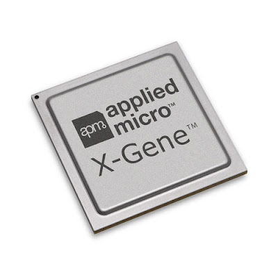
Part of the X-Gene line, the “server-on-a-chip” is a multi-core ARM v8 with L1, l2 and L3 cache, a high-performance memory subsystem, cloud server I/O (Integrated Ethernet and peripheral interfaces), Coherent fabric, SOC peripherals and associated bridges, plus system memory that can host Linux and server software.

"This is the first time the world is seeing a mature, fully-functional server platform running a real-world application on 64-bit ARM-based processor," said Vinay Ravuri, vice president and general manager of processor products at AppliedMicro. 

"As a result, AppliedMicro has already secured key strategic customers and partners around the world and has been enabling them with the tools they need to get started in advance of silicon. This web server emulates a live content delivery application featuring rich video, audio and text, and demonstrates the robustness and readiness of our next generation cloud server solution."

64-bit is a word (natural unit of data used by a particular processor design) size that started being used by PCs in 2003, but has existed in supercomputers since the 1970s and in RISC-based workstations and servers since the early 1990s.

AppliedMicro's newest X-Gene-based servers is expected to get OEMs, ODMs, Cloud Service Providers, Independent Software vendors and other companies to warm up to the idea of ARM-based machinery, after many years of having only x86 (AMD and Intel) to call on.

The high power efficiency continues to be a major asset of the ARM architecture and, with support for essentially all relevant programs now, it should be more convenient than ever to conduct software development, stage performance benchmarking, etc., all the while researching new silicon on the side.


Twitter Delicious Facebook Digg Stumbleupon Favorites More

 
Design by Free WordPress Themes | Bloggerized by Lasantha - Premium Blogger Themes | coupon codes
`