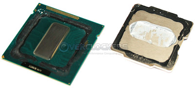
Microprocessor designer and manufacturer, the American/Israeli company Intel, has reportedly admitted that they actually did cut costs on the Ivy Bridge products. The smaller process node led to denser CPU and a hotter die.
Intel still maintains the story that the use of lower quality thermal interface between the CPU dies and the integrated heat spreader was intentional and it is exactly what they’ve planned for.
The company claims that the CPUs will actually pass all certification tests, just as the specifications on their box state.
Intel’s Ivy Bridge comes with a small die and the smaller the die size is, the better the thermal interface with the IHS must be.
If you have a smaller contact area between the IHS and the CPU die, you must make sure that there is improved heat transfer so that the CPU won’t overheat.
Intel figured that if Ivy Bridge has a lower power consumption than Sandy Bridge, they’d practically have less heat to dissipate.
The thing is that, because Ivy Bridge is so dense and the heat transfer is done through a smaller contact area, the heat is not dissipating as fast as it is on Sandy Bride. Therefore, users will have to enjoy a hotter CPU.
We wonder how much money did Intel save by being such a cheapskate and disregarding the best interest of its own customers.
Maybe the sum is considerable and the effort was worth it, but the image backlash in the face of consumers’ dissatisfaction with Intel’s practices will probably prove detrimental overall.


 5/03/2012 07:57:00 PM
 dannzfay


 Posted in:


0 comments:
Post a Comment