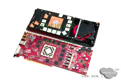
With less than one day separating us from AMD’s release of its Radeon HD 7970 graphics card, the first pictures showcasing the PCB as well as the Tahiti XT GPU used for the HD 7000 series found their way online.
The pictures show both of the card’s printed circuit board as well as the cooling solution employed by AMD, which on the first look seems to resemble pretty much the setup that the company used to chill the HD 6900 series.
There are however a couple of differences that are supposed to improve the airflow provided to the GPU and make the whole setup quitter, but for the most part the two are pretty similar.
Moving to the PCB, the images provided by PC In Life reveal that the card will get its power through a 5+1 phase VRM that is connected to a pair of PCI Express 6-pin plugs.
Together with the PCIe slot, these can deliver up to 225W to the AMD card, which is actually a tad lower than the 250W that AMD is listing under “Maximum Board Power” in the HD 7970 specifications, but I guess that AIBs will equip these with an 6+8-pin config to improve their overclocking potential.
Otherwise, the PCB also gives as a good look at the 3GB of video memory installed using a 384-bit wide bus as well as to the Tahiti XT graphics core.
As we already revealed, this includes 32 Compute Units for a total of 2058 streaming cores, 128 texture units, 32 ROPs and a 384-bit wide memory bus.
We also know that its clock speed is set at 925MHz, while the memory is operating at 1.37GHz (5.5GHz effective).
AMD’s Radeon HD 7970 is expected to be announced on December 22, with availability being scheduled for January of 2012.


 12/21/2011 06:13:00 PM
 dannzfay


 Posted in:


0 comments:
Post a Comment